无监督机器学习:原子分辨图像中的缺陷检测
点击下方卡片,关注“新机器视觉”公众号
重磅干货,第一时间送达
晶体缺陷在决定材料特性方面起着关键作用。例如,二维材料中的点缺陷(如空位和间隙)可以为晶格引入应变并改变电子特性;线缺陷(如位错)和平面缺陷(如 3D 材料中的晶界和孪晶界)可以决定它们的机械性能。晶体缺陷的研究需要原子尺度分辨率的晶体缺陷结构,例如来自扫描透射电子显微镜 (STEM) 图像的晶体缺陷。目前将机器学习 (ML) 应用于电子显微镜的趋势需要“人工智能晶体学家”,它可以自动检测、识别和分析结构特性。基于监督学习的方法可以对缺陷进行检测和分类,它使用来自实验或模拟的人工标记数据来训练模型。这些经过训练的模型通常仅限于训练数据集中的晶体结构,不能轻易推广到其他晶体结构。目前,缺乏一种可靠的无监督机器学习方法来检测 STEM 图像中的晶体缺陷。
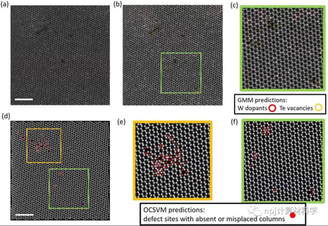
Fig. 1 Results of defect detection in bilayer Mo0.91W0.09Te2.
来自美国橡树岭国家实验室的Lupini和Yueming Guo研究团队,报导了一类支持向量机(OCSVM)来进行晶体缺陷检测,这种方法在工业中广泛用于异常值检测,例如制造和网络安全分析中的快速故障诊断。他们认为晶体缺陷的检测可以转化为一类分类背景下的异常值检测问题。作者引入了两种分割方案来满足具有一类主要数据点的要求:第一种方案适用于广泛的晶体结构,并对晶体对称性施加了限制;第二种方案裁剪傅立叶滤波图像,使每个裁剪图像都以原子列的位置为中心,消除了晶体对称性的限制。为了确保每个子图像中的特征与平移无关,他们将帕特森函数作为特征提取描述符引入了两种方案,使其仅依赖于原子间向量(不包括它们的方向符号)。作者报导的这类方法可用于快速筛选大量 STEM 图像以检测晶体缺陷,还可以改善来自光束敏感材料(例如金属有机框架化合物 (MOF))的噪声原子图像的晶体结构重建。该文近期发表于npj Computational Materials 7: 180(2021)。
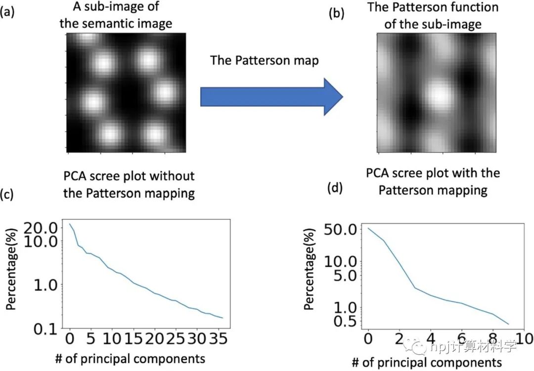
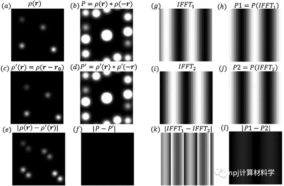
Fig. 2 Illustration of how Patterson mapping can greatly reduce the effect of arbitrary shifts in the fifirst demonstration.
Editorial Summary
Unsupervised ML: Defect detection in atomic-resolution images Crystallographic defects play a key role in defining materials properties. For example, point defects in 2D materials such as vacancies and interstitials can introduce strain to the lattice and modify the electronic properties; line defects like dislocations and planar defects such as grain boundaries and twin boundaries in 3D materials can define their mechanical properties. Studies of crystallographic defects require structural knowledge of crystallographic defects at atomic-scale resolution, such as crystallographic defects from scanning transmission electron microscopy (STEM) images. The current trend of applying machine learning (ML) to electron microscopy demands an ‘AI crystallographer’ that can automatically detect, identify, and analyze structural properties. Previous work demonstrated the detection and classification of defects based on supervised learning methods where human-labeled data from experiments or simulations are used to train the models. These trained models are usually limited to the crystal structures in the training datasets and cannot easily be generalized to other crystal structures. Currently, a reliable method of unsupervised ML for detection of crystallographic defects in STEM images is lacking.
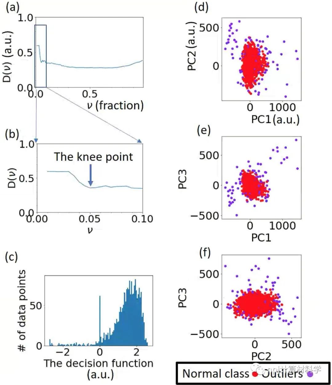
Fig. 3 Details of OCSVM analysis.
A group led by Lupini and Guo from Oak Ridge National Laboratory, USA, proposed the application of the one-class support vector machine (OCSVM), which has been widely used for outlier detection in industry (such as fast fault diagnosis in manufacturing and cyber security analyses), to the detection of crystallographic defects. Such detection of crystallographic defects can be turned into a problem of outlier detection in the context of one-class classification. The authors introduced two schemes of segmentation to satisfy the requirement of having one major class of data points. The first scheme is applicable to a wide range of crystal structures although it imposes limitations to the crystal symmetry. To remove the limitations, they developed a second scheme where they crop the Fourier filtered images and each cropped image is centered at the position of an atom column. To make sure that the features in each subimage are independent of translation, they introduced the application of the Patterson function as a feature extraction descriptor to both schemes, which only depends on the interatomic vectors (excluding the signs of their directions). In this article, the as-reported approach by authors can be applied to rapidly screen a large number of STEM images to detect crystallographic defects, which may be beneficial when analyzing in situ data. Another application is to improve the crystal structure reconstruction from noisy atomic images of beam-sensitive materials such as metal-organic frameworks (MOFs). This article was recently published in npj Computational Materials 7: 180 (2021).
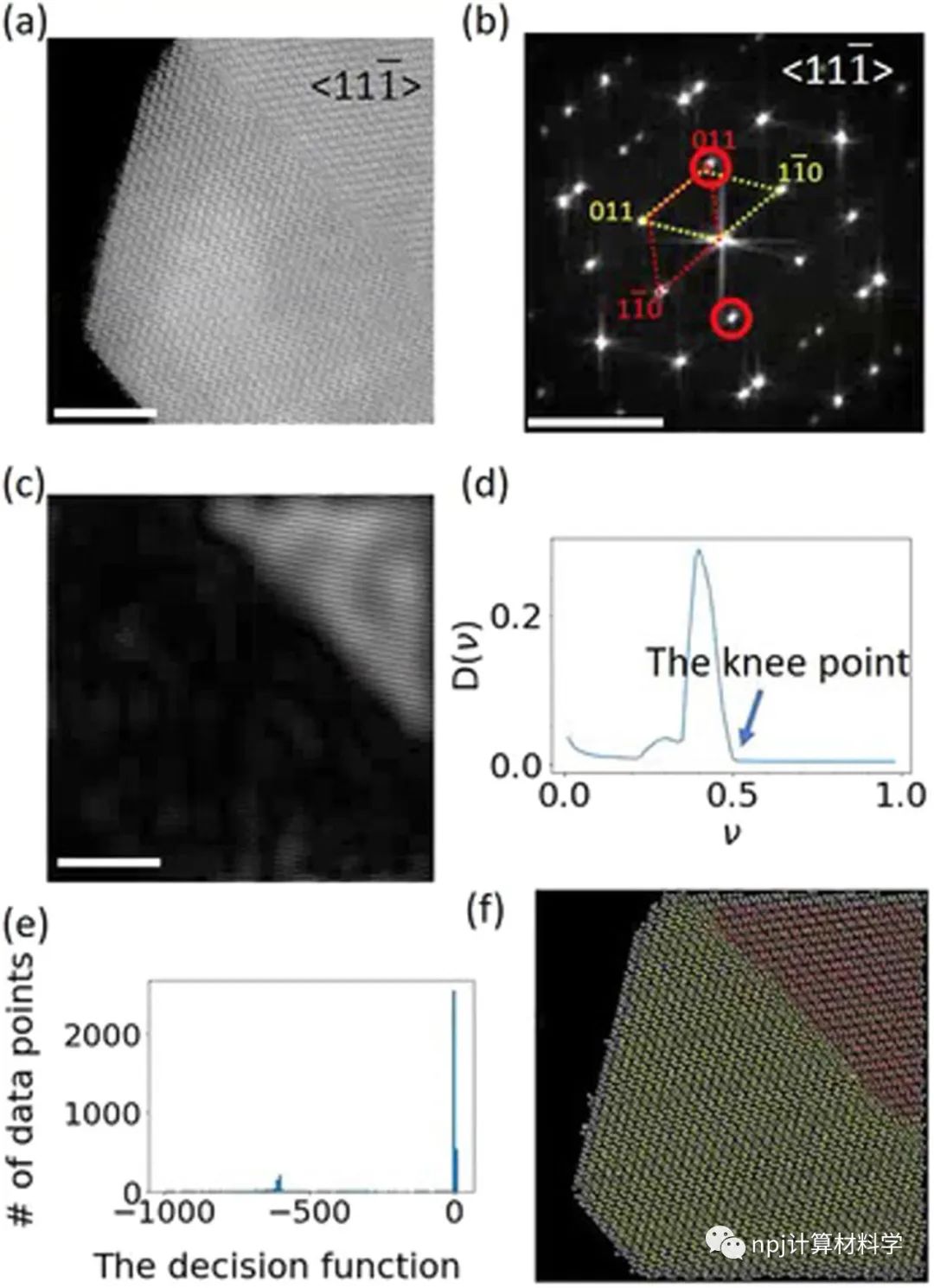
Fig. 4 Demonstration of detecting different domains separated by the twin boundary in a ZrO2 nanoparticle.
原文Abstract及其翻译
Defect detection in atomic-resolution images via unsupervised learning with translational invariance (利用具有平移不变性的无监督学习在原子分辨率图像中检测缺陷)
Yueming Guo, Sergei V. Kalinin, Hui Cai, Kai Xiao, Sergiy Krylyuk, Albert V. Davydov, Qianying Guo & Andrew R. Lupini
Abstract Crystallographic defects can now be routinely imaged at atomic resolution with aberration-corrected scanning transmission electron microscopy (STEM) at high speed, with the potential for vast volumes of data to be acquired in relatively short times or through autonomous experiments that can continue over very long periods. Automatic detection and classification of defects in the STEM images are needed in order to handle the data in an efficient way. However, like many other tasks related to object detection and identification in artificial intelligence, it is challenging to detect and identify defects from STEM images. Furthermore, it is difficult to deal with crystal structures that have many atoms and low symmetries. Previous methods used for defect detection and classification were based on supervised learning, which requires human-labeled data. In this work, we develop an approach for defect detection with unsupervised machine learning based on a one-class support vector machine (OCSVM). We introduce two schemes of image segmentation and data preprocessing, both of which involve taking the Patterson function of each segment as inputs. We demonstrate that this method can be applied to various defects, such as point and line defects in 2D materials and twin boundaries in 3D nanocrystals.
Fig. 5 Demonstration of applying Patterson function to provide translation-invariant features in segmented subimages.
摘要 现在可以通过像差校正的扫描透射电子显微镜 (STEM) 以原子分辨率对晶体缺陷进行高速成像,并有可能在相对较短的时间内或通过可以持续很长时间的自主实验获得大量数据。为了能够以有效的方式处理数据,需要对 STEM 图像中的缺陷进行自动检测和分类。然而,与人工智能进行物体检测和识别任务一样,从 STEM 图像中检测和识别缺陷具有挑战性。此外,处理具有许多原子和低对称性的晶体结构是有难度的。以前用于缺陷检测和分类的方法是基于监督学习,需要人工标记数据。在本工作中,我们开发了一种基于一类支持向量机 (OCSVM) 的无监督机器学习缺陷检测方法。我们介绍了图像分割和数据预处理两种方案。这两种方案都涉及将每段的帕特森函数作为输入。我们证明了这种方法可以应用于各种缺陷,例如 2D 材料中的点和线缺陷以及 3D 纳米晶体中的孪晶界。
转自:npj计算材料学
本文仅做学术分享,如有侵权,请联系删文。
